ADVANCED SEMICONDUCTOR & ELECTRONIC PROCESS MATERIALS
Advanced Semiconductor & Electronic Process MaterialsEnabling High-End Manufacturing
High-performance adhesive materials, functional films and process solutions for semiconductors, advanced packaging, IC substrates and PCB/FPC manufacturing.
Solutions
SOLUTIONS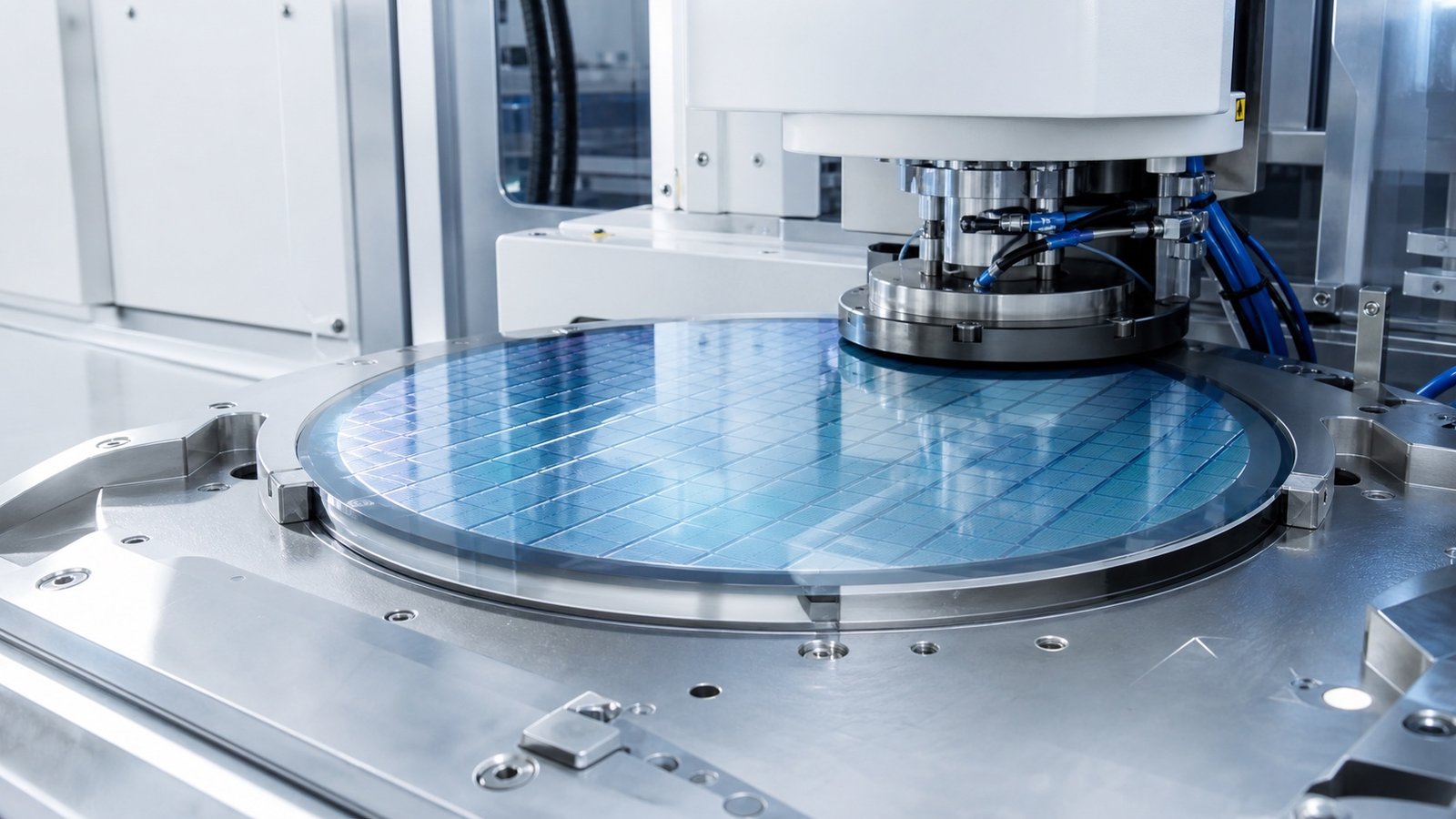
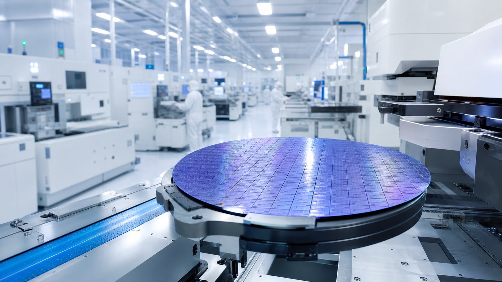
01Semiconductor Manufacturing半导体制造
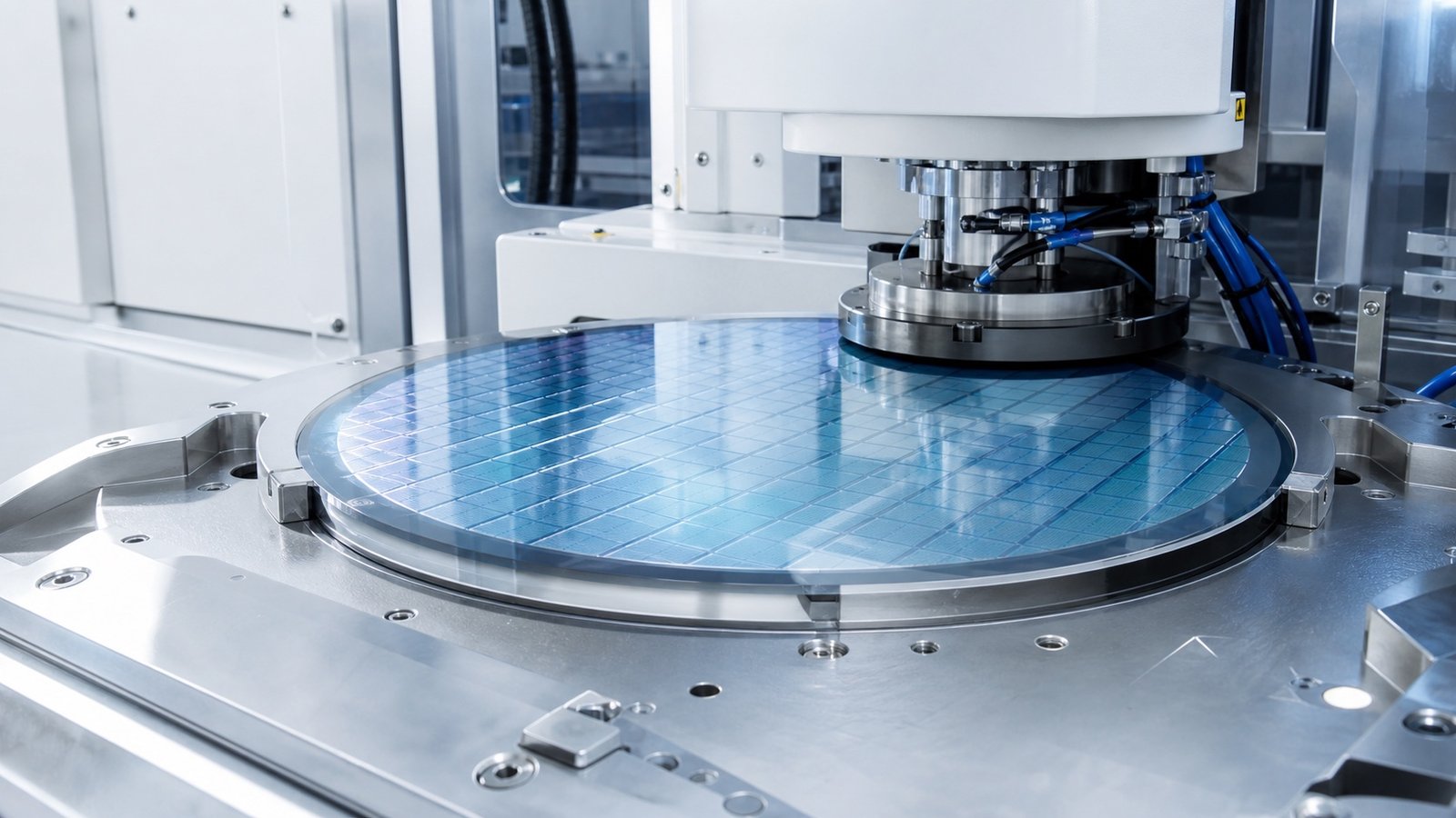
Validated functional tapes and protection materials for wafer back grinding, dicing and surface protection.
→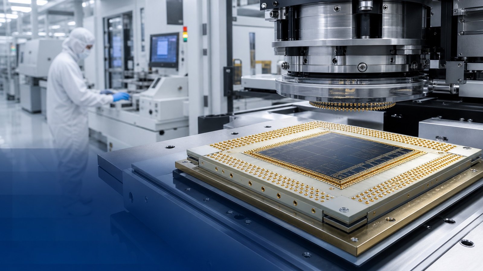
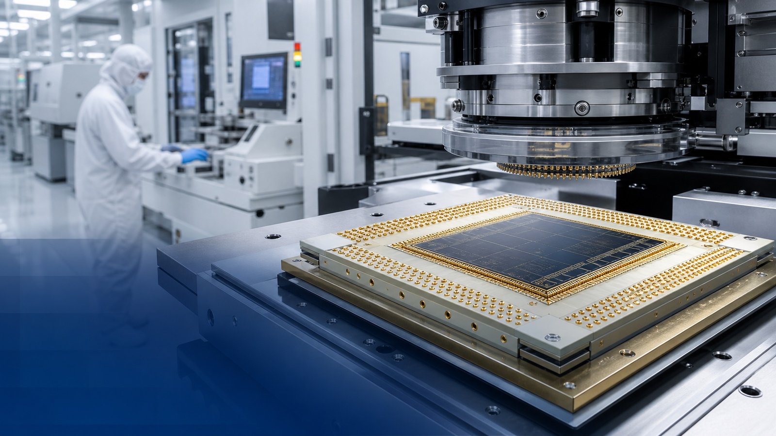
02Advanced Packaging先进封装
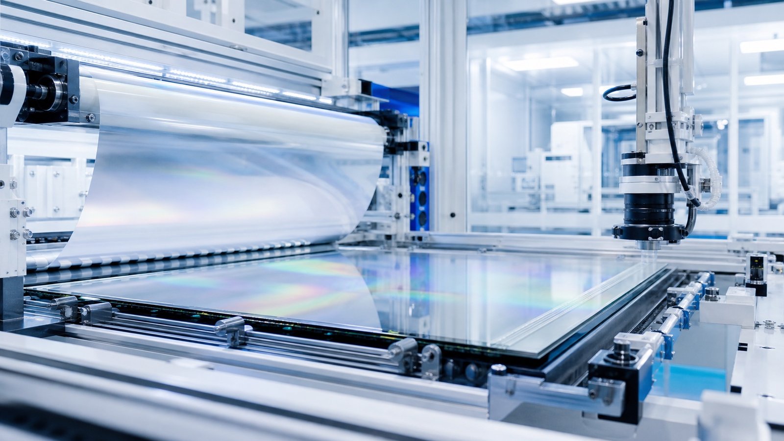
Material matching and application validation for die attach, package dicing and temporary fixing processes.
→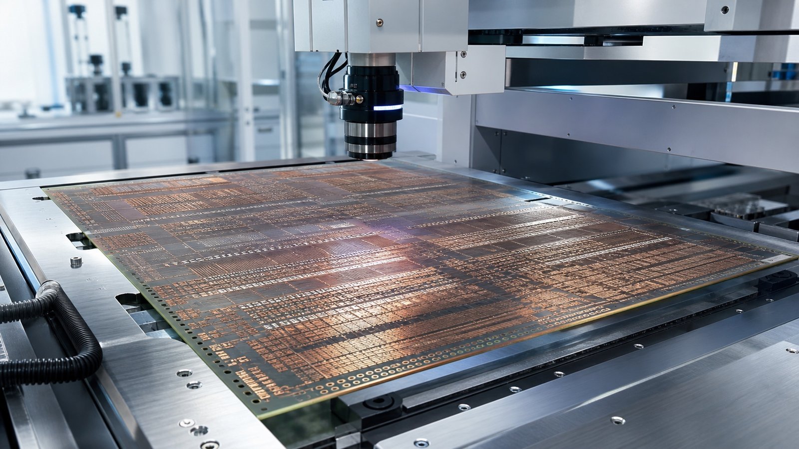
03IC SubstrateIC载板
Materials for substrate dicing, elevated-temperature processes and surface protection in fine-line manufacturing.
→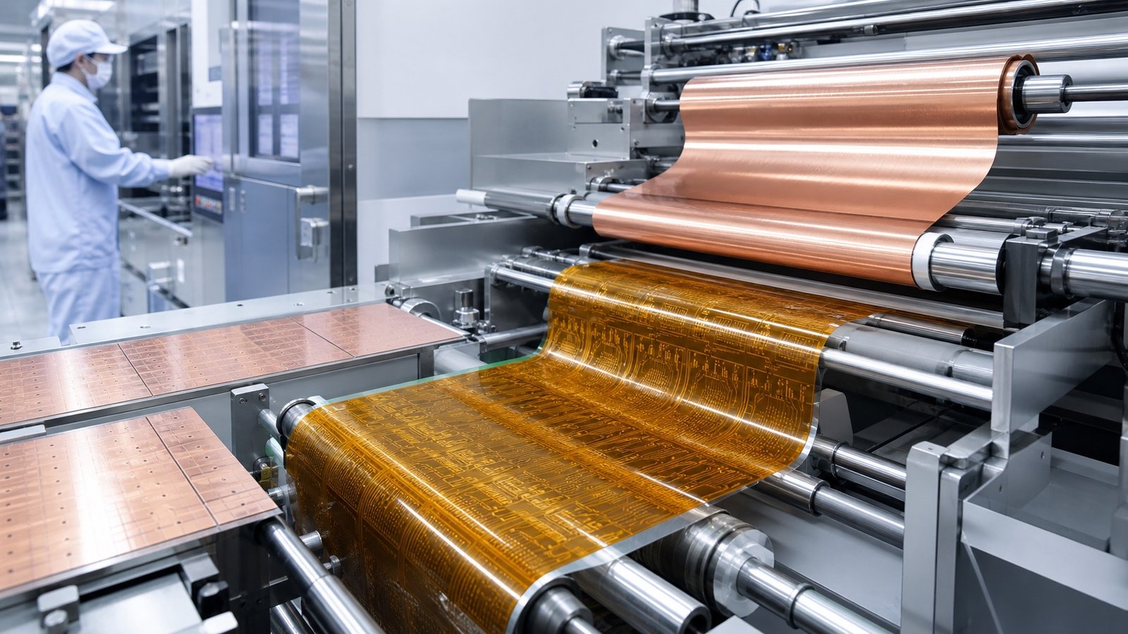
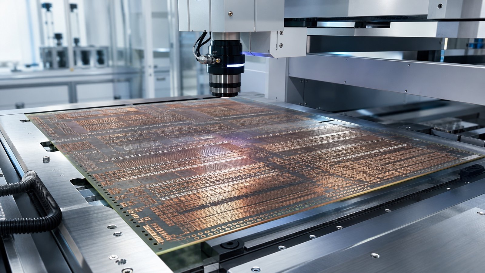
04PCB & FPC ManufacturingPCB / FPC制造
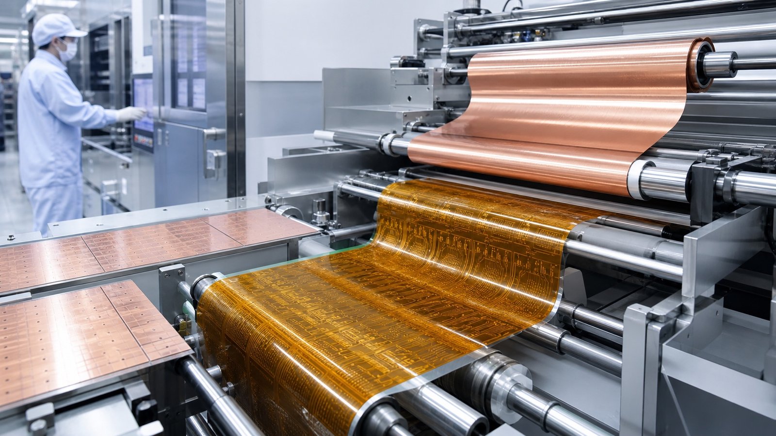
Material portfolios and application support for plating, high-temperature processing, protection and precision lamination in PCB and FPC manufacturing.
→Product Center
PRODUCT CENTER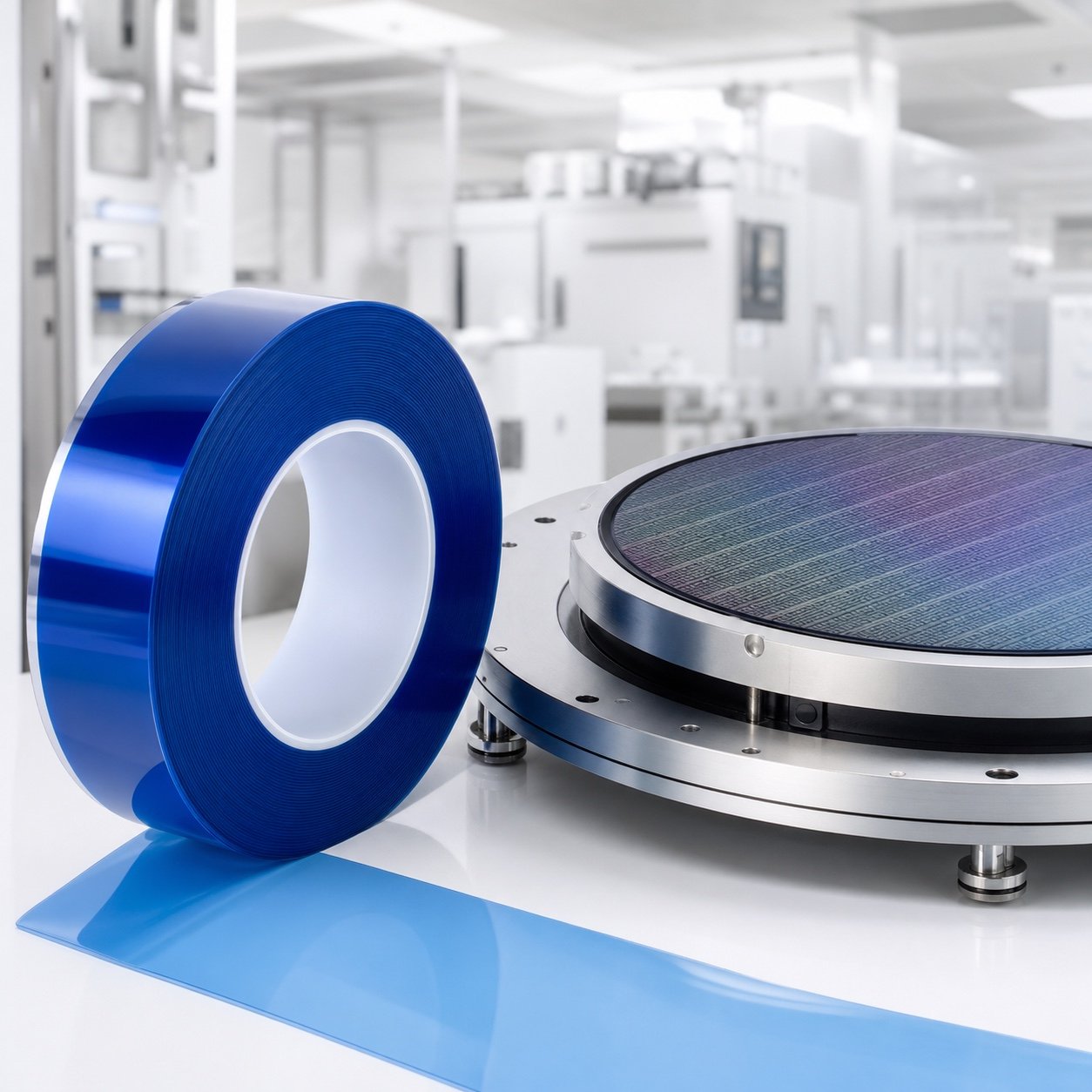
Back Grinding Tape背磨胶带Semiconductor→
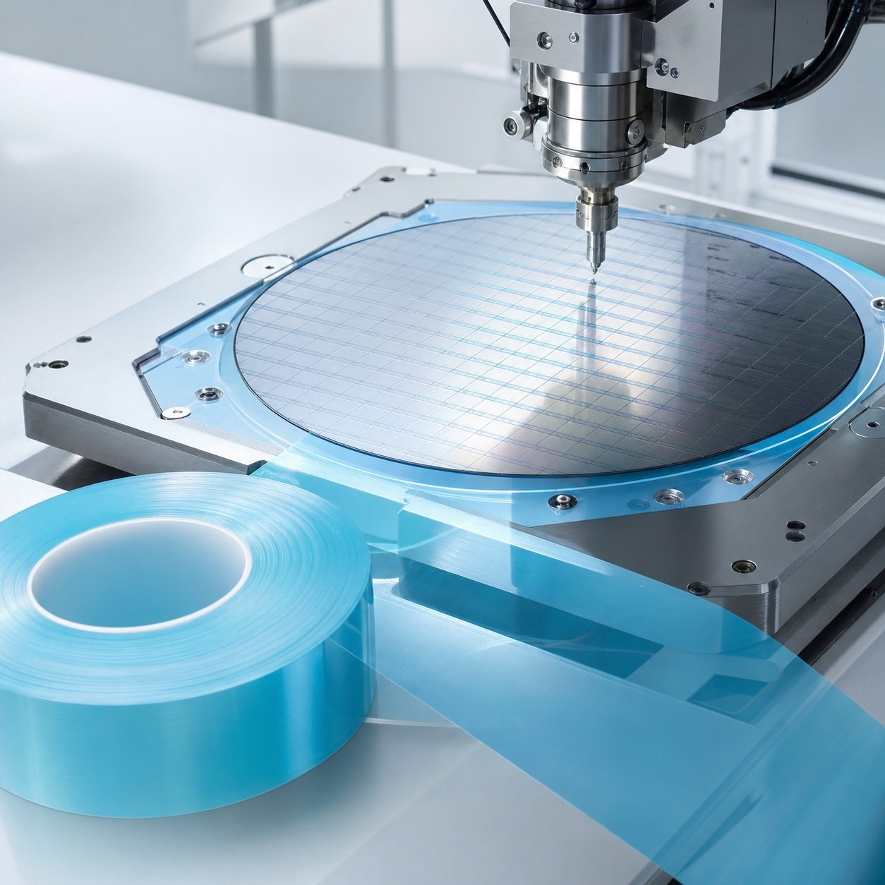
Wafer Dicing Tape晶圆切割胶带Semiconductor / Advanced Packaging→
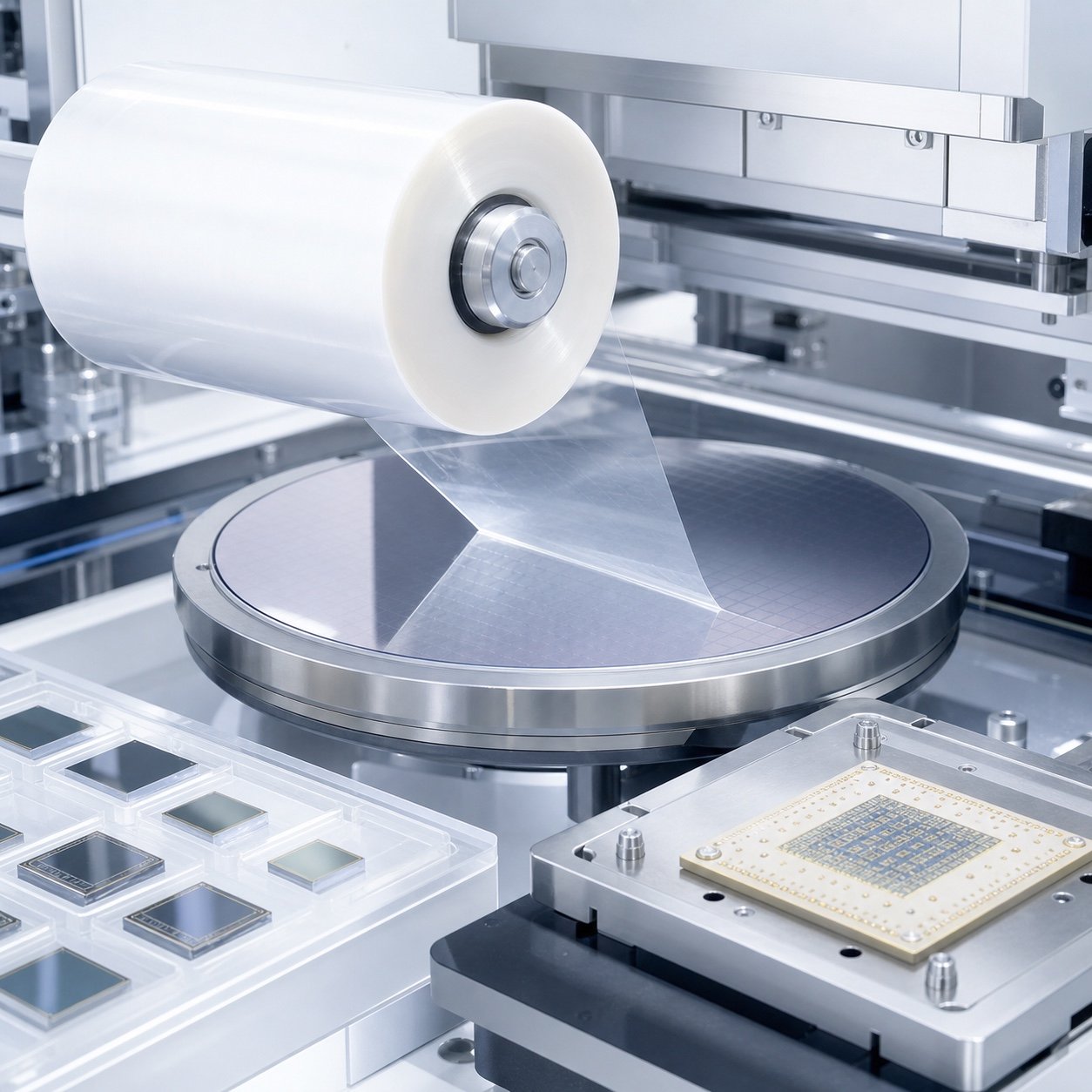
Die Attach Film (DAF)芯片贴装膜(DAF)Advanced Packaging→
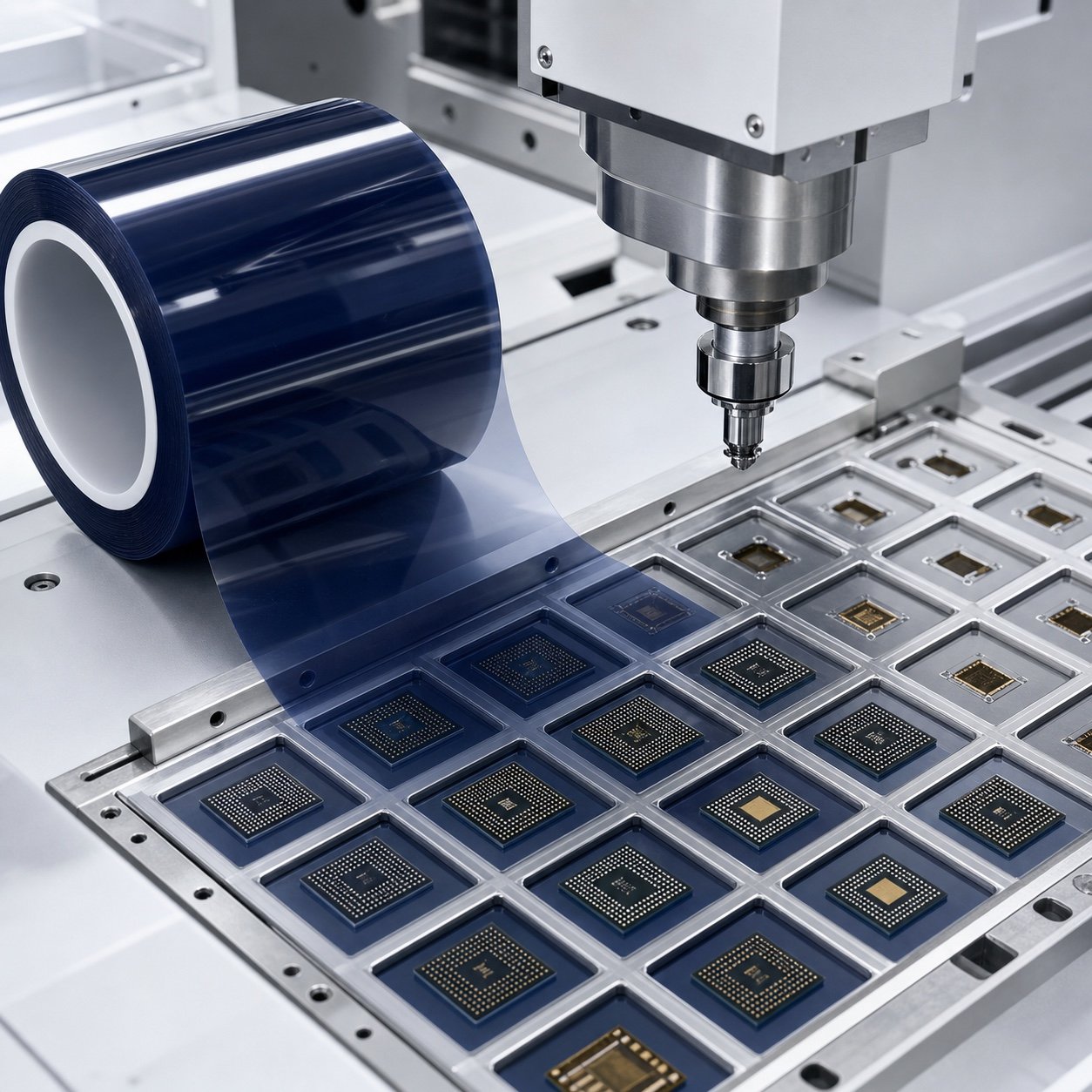
Package Dicing Tape封装切割胶带Packaging / IC Substrate→
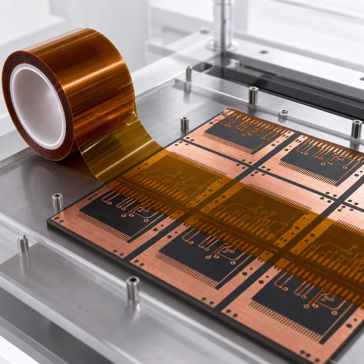
Heat Resistant Tape (PI)耐高温胶带(PI)Semiconductor / PCB / FPC→
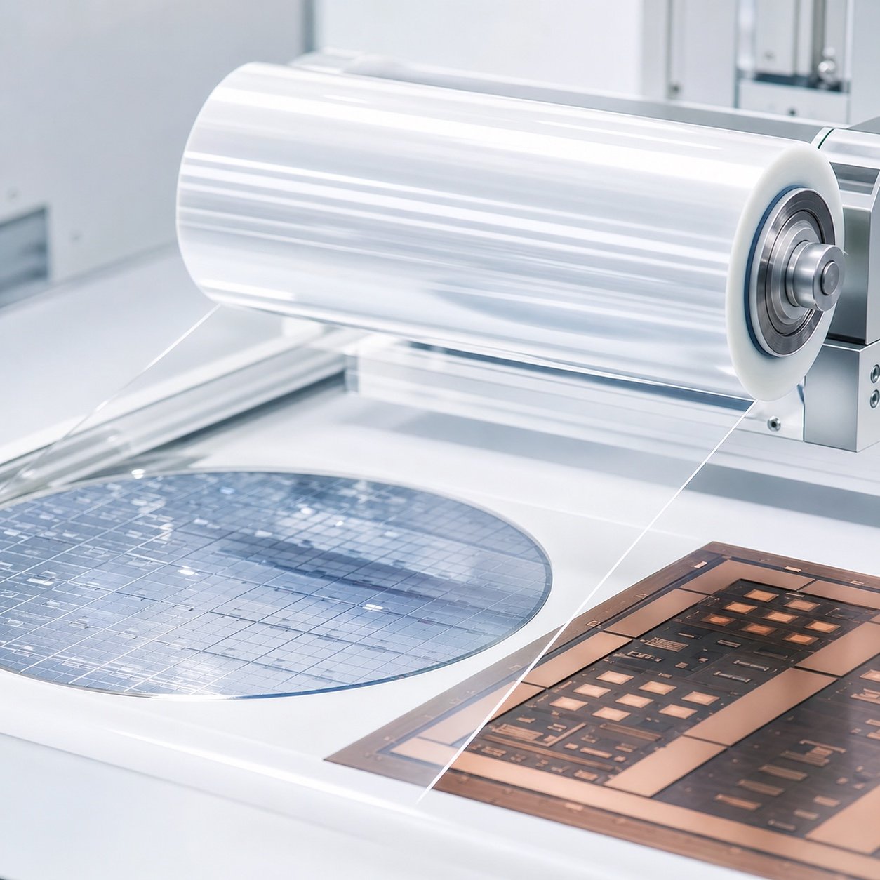
Process Protection Film制程保护膜Semiconductor / PCB→
Technology & Innovation
TECHNOLOGY & INNOVATIONMaterial Technology for Advanced Processes
Continuous development of adhesive systems, functional films and process compatibility supports the cleanliness, reliability and stability demanded by advanced manufacturing.
01Material Engineering材料研发
02Adhesive Technology胶黏技术
03Process Compatibility制程兼容
04Application Validation应用验证

Quality Assurance
QUALITY ASSURANCE01Incoming Inspection原材料检验→
02Process Control制程控制→
03Performance Testing性能测试→
04Batch Traceability批次追溯
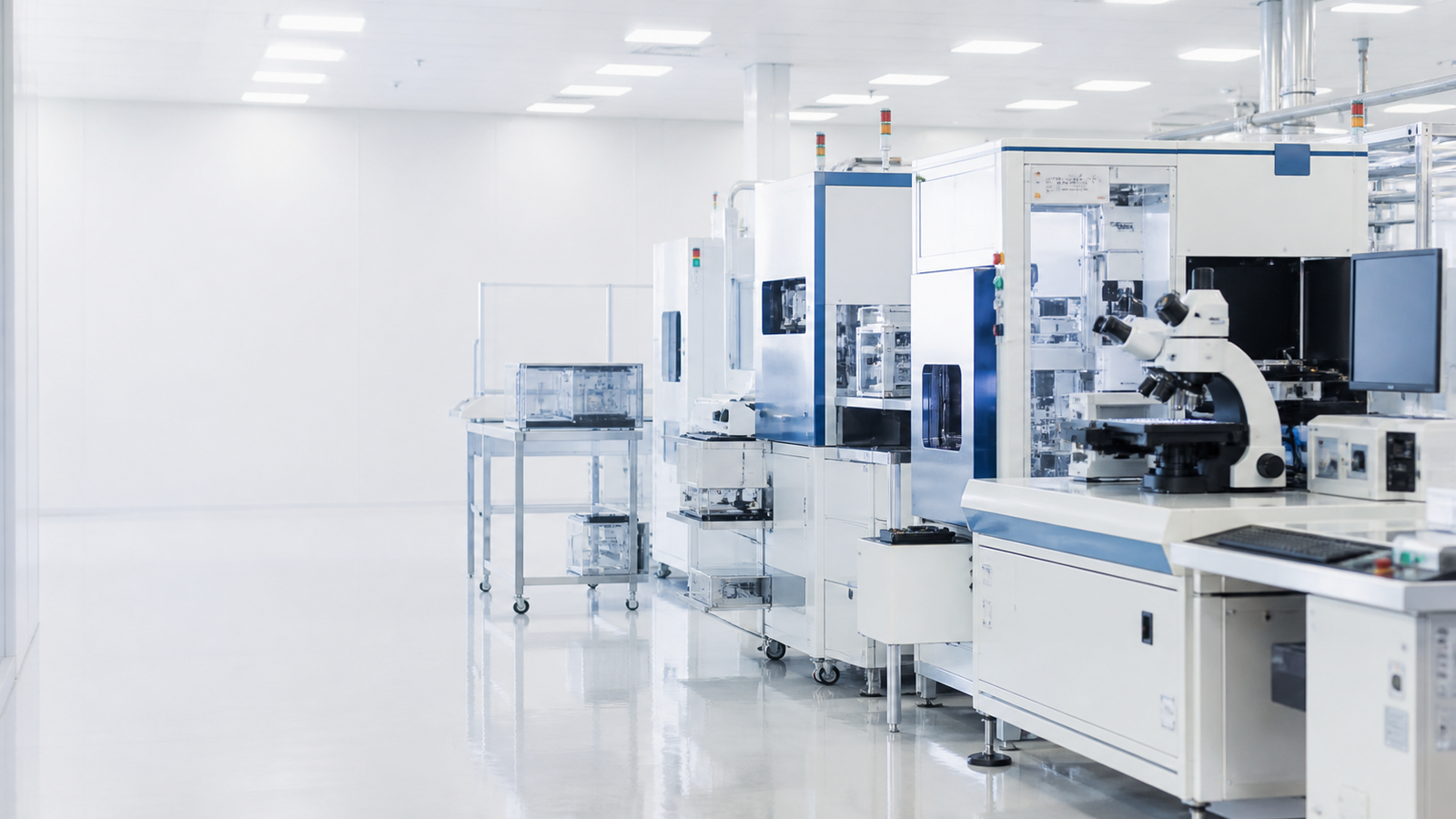 Process-wide quality control
Technical Insights
TECHNICAL INSIGHTS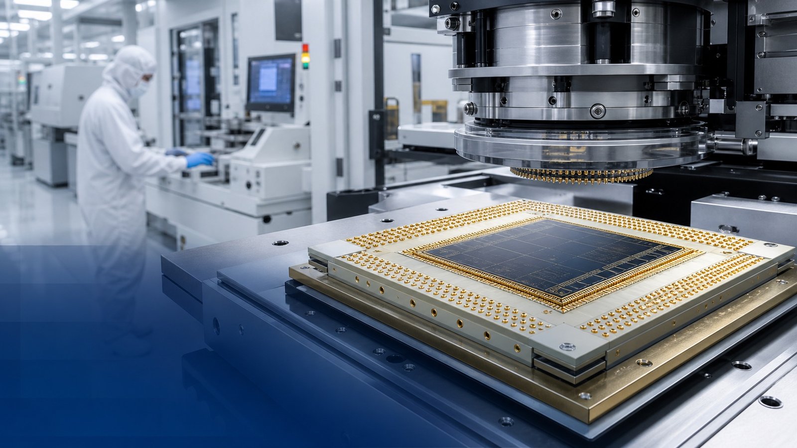
Performance requirements for functional adhesives in advanced packaging
Read More →